Silicon wafer quality defines everything downstream of it. A single hidden micro-crack that escapes inspection will propagate through cell processing, module lamination, and field operation before surfacing as a warranty claim years later. The traditional response — statistical sampling at 1–2% — made economic sense when line speeds were 2000 pcs/h and crack widths of 30 micrometers were the main concern. Neither condition holds in 2026.
Why Sampling Fails at Modern Line Speeds
Today's tier-one wafer lines run at 5000–7000 pieces per hour. At those speeds, sampling-based inspection has three fatal limitations:
- Escape rate: Even at 2% sampling, 98% of cracks leave the line unexamined. A single escaped wafer with an edge micro-crack can cause a 3–5 cell cascade during lamination.
- Root cause lag: Process drifts (diamond wire wear, water jet pressure changes, transport shock) only show up in sampling data hours after they begin, by which time tens of thousands of wafers have been produced.
- Traceability gaps: Customers increasingly demand individual-wafer traceability. Sampling cannot provide it.
The industry has responded with full-line inline inspection. The economic calculation that once favored sampling has reversed — the cost of a single warranty claim now exceeds the amortized capital cost of an inline system.
The 6000 pcs/h Throughput Challenge
Running 100% inspection at 6000 pieces per hour gives each wafer approximately 600 milliseconds of sensor time. Within that window the system must:
- Position the wafer precisely without contact damage
- Excite luminescence (EL via contact probes or PL via laser)
- Capture a full-area high-resolution image
- Run defect classification (typically AI-based)
- Communicate a pass/fail decision to the handler
Each step carries its own engineering complexity. Contact probing at production speed must avoid micro-damage that itself becomes a crack. Laser-excited PL eliminates contact but requires careful thermal management to keep wafers below 40 °C during the measurement.
Sensor and Optics Requirements
Production-grade inline systems typically use:
- InGaAs sensors in the 900–1700 nm range to capture the silicon bandgap emission
- Minimum 12-megapixel resolution to resolve cracks below 3 micrometers at full wafer field of view
- Global shutter operation to prevent motion blur at transport speeds
- Dynamic range ≥70 dB to handle both bright active areas and dark crack signatures in one frame
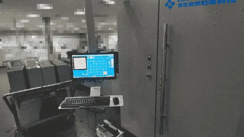
The SC-MC-W inline wafer inspection module from Vision Potential implements this stack and has been validated at production lines running up to 6000 pcs/h with full traceability integration into MES systems.
Defect Categories Captured
A properly configured inline system identifies:
- Micro-cracks (transverse, longitudinal, radial, edge)
- Chipping along cut edges
- Sawing marks from diamond wire wear
- Breakage from handler mishandling
- Stress concentration zones (pre-crack warnings)
- Resistivity anomalies that predict cell efficiency spread
Modern AI classifiers running on GPU inference nodes achieve detection rates above 99.5% for cracks larger than 5 micrometers, with false-positive rates below 0.3% when trained on 500,000+ production images.
Economics: ROI in 8–14 Months
A 3 GW/year wafer line processing roughly 500 million wafers annually derives the following from 100% inspection:
| Value Driver | Annual Benefit |
|---|---|
| Reduced cell line scrap | 0.4–0.7% yield recovery |
| Warranty claim reduction | 30–60% fewer field failures traced to wafer origin |
| Process improvement | 15–25 minutes faster drift detection |
| Customer premium | 2–4% price premium for traceable wafers |
At typical industry economics, the payback period for a dual-module inline inspection investment is 8–14 months on a 3 GW line.
What to Specify When Procuring
Fab operators evaluating inline systems should verify:
- Sustained throughput benchmark at the actual wafer format to be produced (M10, G12, G12R)
- Detection statistics measured on defect reference wafers, not proprietary test panels
- Integration protocol with existing MES (typically OPC-UA or direct SQL)
- Classifier retraining workflow — labeling tools, retraining frequency, validation protocol
- Service response time and spare parts inventory for the specific sensor model
Forward Outlook
As the industry transitions to thinner wafers (130 μm and below for HJT) and larger formats (G12, G12R), the crack profiles themselves are shifting. Thinner wafers show more radial stress cracks, larger wafers show more handling damage at the corners. Inline inspection systems need upgrade paths — configurable optics, retrainable classifiers, flexible handlers — rather than being locked to today's defect library.
100% wafer crack inspection is no longer a premium tier differentiator. It is the new production baseline, and fabs without it carry a silent but growing warranty exposure.