
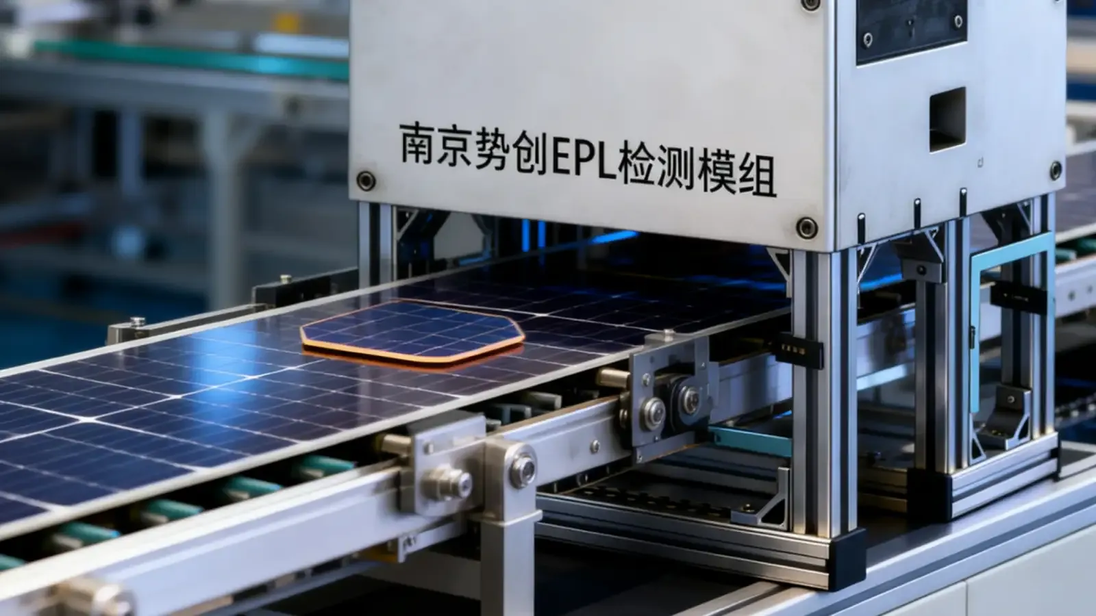
Birth Certificate for Raw Wafers: SC-SPL PL Module Catches Defects Before Slicing
In PV manufacturing, raw wafers are the most fundamental yet most overlooked checkpoint — most customers only do post-slice dimensional checks, with no method to inspect internal defects. The consequence: wafers carrying internal dislocations, contamination, or grain-boundary anomalies still get sliced, edge-ground, cleaned and fed into the cell line — only the cell-line EL inspection finally catches them, by which point you've already lost $0.11/wafer in processing cost. SC-SPL Raw-Wafer PL Module pushes inspection upstream of slicing, giving wafers a true "birth inspection".
1. Why raw wafers need their own inspection
A common question: "If we already inspect ingots, doesn't that cover wafers?" Not quite. Ingot-to-wafer transition crosses two high-risk steps:
- Multi-wire cutting: high-speed diamond-wire cutting introduces mechanical and thermal stress, leaving micro-damage on/in the wafer;
- Edge grinding / cleaning: grinding force + chemical etch can migrate previously-buried impurities to the wafer surface.
Wafer-stage defect rate is typically 1.5–2× higher than ingot-stage, and the increment can only be detected at the wafer level.
2. Physical challenges of raw-wafer inspection
Compared to cell inspection, raw wafers bring three unique challenges:
| Challenge | Raw wafer | Cell |
|---|---|---|
| Electrodes | None | Full electrodes |
| Surface | No passivation, high reflectance | Passivated |
| Thickness | 130–180 µm | 130–180 µm |
| Excitation options | PL only (no electrode) | EL / PL / EPL |
| Signal strength | 30–50% weaker than cells | Stronger |
The crucial difference: no electrodes — EL/EPL are unavailable, PL is the only option. That means the PL system must be more sensitive and more stable.
3. Three core technologies in SC-SPL
3.1 Total-internal-reflection PL excitation
Bare wafers reflect 35% of incident light. Conventional PL wastes much of the laser energy on reflection. SC-SPL uses total-internal-reflection PL excitation: the laser enters the wafer near the critical angle through a specialized optical element, gets trapped via total internal reflection, and excites the wafer multiple times. This boosts wafer PL signal strength by 1.8–2.4×.
3.2 Multi-band PL signal extraction
Crystalline-silicon PL emission peaks near 1100 nm, but defects shift the peak slightly:
- Dislocations: 1080–1090 nm
- Contamination: 1110–1120 nm
- Stress regions: 1095–1105 nm
SC-SPL adds three narrowband tunable filters in front of the InGaAs camera, capturing images at the three feature wavelengths and fusing them. This raises classification accuracy from 87% (single-band) to 96.5% (three-band fusion).
3.3 High-speed contactless conveyance
Wafers in slicing workshops scratch easily; conventional contact belts won't do. SC-SPL ships with an air-bearing conveyance platform: wafers float on 0.05 MPa positive air pressure with zero physical contact, at 0.8–1.2 s/wafer cycle.
4. Optimal deployment location
SC-SPL's best deployment is between the slicer outlet and the cleaner inlet:
Slicer → Buffer → SC-SPL inspection → Defect routing →
  Pass → Cleaner → Stock
  Fail → Re-cut (if thickness allows) / Scrap
Two benefits:
- Early loss containment: defective wafers skip cleaning, saving water/chemicals;
- Data feedback: defect distribution back-traces to specific saw lines and parameters, pinpointing the root cause within 2–3 days.
5. Customer scenarios and ROI
A GCL granular-silicon plant's 90-day data after deploying SC-SPL:
| Metric | Before | After |
|---|---|---|
| Wafer-stage defect interception | 0% (no inspection) | 96% |
| Downstream cell EL defect rate | 6.8% | 2.1% |
| Monthly scrap value | $540K | $130K |
| Slicer parameter tuning cycle | 7–14 days to spot issue | 2–3 days to localize |
Net monthly savings: ~$410K, payback in ~4 months.
6. The data value of "wafer birth certificates"
SC-SPL is more than an inspection tool — it is the entry point of raw-wafer data assets. Per-wafer defect distribution, stress maps, and impurity types all upload to MES and integrate with downstream cell and module data:
- Wafer-level traceability: when a module fails, backtrace to the wafer batch in 30 minutes;
- AI process optimization: massive wafer data trains AI to recommend optimal slicer parameters;
- Insurance & warranty: wafer birth certificates underpin long-term reliability studies.
For an SC-SPL demo or a slicer-integration evaluation, contact MVCreate at +86 159-5048-9233.
Originally published by Vision Potential (Nanjing MVCreate Intelligent Technology Co., Ltd.). Reproductions must credit the source.